


About Us
Executive Editor:Publishing house "Academy of Natural History"
Editorial Board:
Asgarov S. (Azerbaijan), Alakbarov M. (Azerbaijan), Aliev Z. (Azerbaijan), Babayev N. (Uzbekistan), Chiladze G. (Georgia), Datskovsky I. (Israel), Garbuz I. (Moldova), Gleizer S. (Germany), Ershina A. (Kazakhstan), Kobzev D. (Switzerland), Kohl O. (Germany), Ktshanyan M. (Armenia), Lande D. (Ukraine), Ledvanov M. (Russia), Makats V. (Ukraine), Miletic L. (Serbia), Moskovkin V. (Ukraine), Murzagaliyeva A. (Kazakhstan), Novikov A. (Ukraine), Rahimov R. (Uzbekistan), Romanchuk A. (Ukraine), Shamshiev B. (Kyrgyzstan), Usheva M. (Bulgaria), Vasileva M. (Bulgar).


Engineering
 PDF
PDFIn studies [1, 2] spatial film sensors for structural surface crack monitoring, based on electrical impedance tomography technic and thin conductive film net, commutated by triacs were proposed. That sensors were designed based on the principle that the electronic properties of film, such as conductivity, change when film is damaged. Spatial film sensor is applied to structural surface and represents itself layered structure that consists of thin conductive film – sensitive element, and thin dielectric film electrically insulates sensitive element from object of control.
The purpose of the present work is to investigate connection between the stress-strain state of the structure (aluminum substrate) contains crack and the stress-strain state of the sensitive element. It is important to show that value of stress, arising in thin conductive film under crack is enough for defect registration.
For the purpose discussed above in this paper elasto-plastic tension two-dimensional problem of rectangular sample with a crack and spatial film sensor on its top edge is considered. The commercial software ANSYS is used for the numerical simulation. It is assumed that adhesion between sensitive film and dielectric film, and dielectric film and structural surface is ideal. Mechanical properties of adhesive are not taken into consideration. The solution is got for the sectional shape shown in Fig. 1 and for the following dimensional and applied pressure value: l = 5 mm, h = 1 mm, hcrack = 200 mkm, h2 = 70 mkm, h1 varying from 10 mkm to 70 mkm and σ = 10 MPa. Bending and pressure were directly applied on the substrate as shown in Fig.1. The mechanical properties (Young’s modulus E, Poisson’s ration, and density) of the structural elements of the model are listed in Table 1.
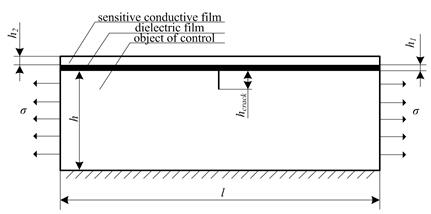
Fig. 1. Geometry of the model
Table 1. Mechanical properties
The model that shown in Fig. 1 has a plane of symmetry that lies on crack profile. So, half of the model was considered, and appropriate boundary condition was set.
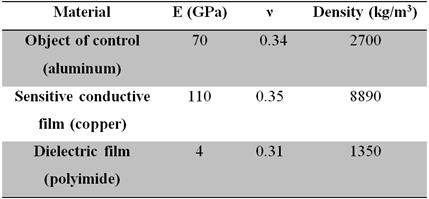
The von Mises stress distribution in the layered structure and substrate under bending and tensile static loadings are shown in Fig. 2.
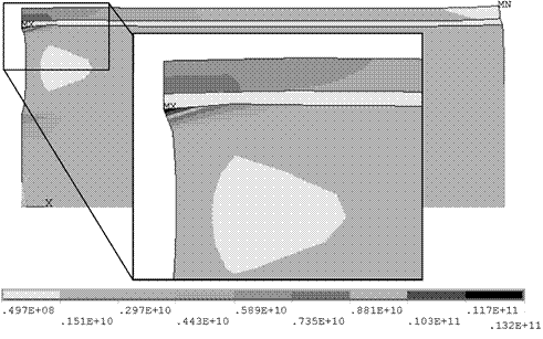
Fig. 2. Results of the layered structural and substrate with a crack finite element analysis under bending and tensile static loadings
The relation between von Mises stress and maximum stress in sensitive conductive film and thickness of polyimide film is shown in Fig. 3. The distribution of von Mises stress in sensitive conductive film in nodes above the crack is shown in Fig. 4.
Fig. 3. The relation between von Mises stress and maximum stress in sensitive conductive film and thickness of polyimide film
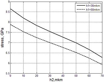
Fig. 4. The distribution of von Mises stress in sensitive conductive film
These simulation results show that the stresses appear in sensitive film strictly depend on dielectric film thickness. It is important to notice that in dielectric film stresses are minimal, so polyimide is an appropriate material for the goal of defect control sensor design. The disruption should be occurring first in sensitive film, otherwise sensor data would be incorrect. Simulation also allows to predict the value of maximum stresses zone in sensitive film, so the resolution of the sensor could be evaluate. These modeling results proves the possibility of detection surface defects, such as cracks, under the tensile stress that normal to the plane of the crack, in case of optimal films thickness choosing and taking into account the mechanical properties of dielectric film.
This study was supported by the Ministry of Education and Science of Russian Federation (project 213.01–11/2014–12).
2. A.S. Isaeva, ‘The method of crack detection based on spatial sensor’ // International scientific conference «Nanotechnologies-2012» – Taganrog: SFEDU, 2012. –pp.120 – 121.
Konoplev B.G., Isaeva A.S., Ryndin E.A. ANALYSIS OF THE STRESS-STRAIN STATE OF THIN FILM SENSOR IN A LAYERED STRUCTURE WITH A CRACK. International Journal Of Applied And Fundamental Research. – 2014. – № 3 –
URL: www.science-sd.com/458-24590 (12.04.2026).