


About Us
Executive Editor:Publishing house "Academy of Natural History"
Editorial Board:
Asgarov S. (Azerbaijan), Alakbarov M. (Azerbaijan), Aliev Z. (Azerbaijan), Babayev N. (Uzbekistan), Chiladze G. (Georgia), Datskovsky I. (Israel), Garbuz I. (Moldova), Gleizer S. (Germany), Ershina A. (Kazakhstan), Kobzev D. (Switzerland), Kohl O. (Germany), Ktshanyan M. (Armenia), Lande D. (Ukraine), Ledvanov M. (Russia), Makats V. (Ukraine), Miletic L. (Serbia), Moskovkin V. (Ukraine), Murzagaliyeva A. (Kazakhstan), Novikov A. (Ukraine), Rahimov R. (Uzbekistan), Romanchuk A. (Ukraine), Shamshiev B. (Kyrgyzstan), Usheva M. (Bulgaria), Vasileva M. (Bulgar).


 PDF
PDFIntroduction of advanced technologies advances the necessity for more up-to-date science structural and social organizational forms, integrating academic education, research and entrepreneurship into a unified complex. In addition, all nanotechnologies have some impact on consumers. An important research problem for effective use ofnanotechnologies in agriculture is development and applications of the new type of high performance low cost thermoelectric modules (TEM), assessment of the possibility to acquire in the process of production dependable information on all the attributes of a product, which affect its quality.
The purpose of the research is design and scientific providing of new type of high performance low cost thermoelectric modules. The research relates to Peltier effect thermoelectric devices, namely to thermoelectric generators, thermoelectric heating and cooling devices and more particularly to the thermoelectric modules as units of such devices based on Peltier and Seebeck effects.
An object of the present research is therefore to provide the thermoelectric module of said type achieving improved the manufacturing process of permanently connecting plates made of thermally and electrically conductive material with intermediate elements pre-connected to thermoelectric semiconductor elements.
As a result of experimental researches, optimal parameters of thermoelectric module and their thermoelectric semiconductor elements were scientifically defined and justified.
Keywords: thermoelectric module, Peltier and Seebeck effects.
INTRODUCTION
The world’s governments currently spend 10 billion USD per year on nanotechnology researchand development, with that figure set to grow by 20 % over the next three years. Latvia allocated 0.4 million Euro to nanotechnology development through its science budget. Latvia had the lowest rate of publication of nanotechnology research in Europe with 0.31 publications per100,000 residents (7 articles) compared to Estonia with 2.91 (39 articles) and Switzerland with 13.39 (1,031 articles). Latvia is likely to become ahotbed of activity for development of “apps” that utilize the platform technology developed by the US or other large markets. In relation to significance of nanotechnology in agriculture and food production nanotechnology promises to improve yields with reduced use of fertilizers, energy inputs, herbicides and other pesticides. (Moskvins et al, 2012).
Therefore goal of research is design and scientific providing of new type of nano structured thermoelectric modules (TEM) to gain at least 10% of the world markets of thermoelectric products. For this purpose the production of thermoelectric modules for milk thermoelectric coolers and generators,highperformance low cost TEM elementswill be realized. These new TEM will gradually replace the existing products on the market. For the achieving this objective, has been new type of TEM elaborated, which have a wide range of applications in industry as well as in agriculture. New type of TEM will improve consumer properties of products and will reduce content of rare earth elements (g/W of the power of TEM).
In present research is used the Peltier and Seebeck effect, thermoelectric semiconductor elements, the thermally and electrically conductive materials, thermoelectric coolers (TEC) and thermoelectric generators (TEG). The former is a device that generates thermal cold and heat by feeding a current to go through TEC. The latter is also a device that generates electrical voltage potential, and thus electrical current after adding an electrical load, by creating a thermal temperature difference between the 2 sides of the TEG. Generating thermal cold and heat from electrical current is called Peltier effect.
Latvia has significant potential in such area of energetics as, for example, the photovoltaic systems for improved distributed energy systems needed for rural development. In relation to significance of nanotechnology in agriculture, nanotech promises to improve the energy efficiency of equipment and will significantly reduce loss of energy. Furthermore, application of nanotechnology in the production of thermoelectric modules for milk thermoelectric coolersis a user-friendly approach to the environment and farm animals.
Objective of improving the quality characteristics of TEM:Reduction of the rare earth elements in TEM (g/W) of at least 80%; Improve consumer properties of TEM: temperature resistance, resistance to cyclic loads, increased efficiency (COP); Market entry of the new generation of TEM: large in size planar dimensions, the increased density of the heat flow, multi-variant voltage, low thickness, improved performance ratio of the mass to the dimensions; Market entry of the thermoelectric panels and multi-stage modules that do not have analogues in the world, as well as a combination of thermoelectric panels and panel cascading inserts that provide a significant local temperature decrease.
Objective of improving the quality of technology: Reduction of the cost of TEM by not less than 50%; Reduction of the material technology by 50%; Reduction of the energy consumption of the process; Development of the technology has based on the use of the most efficient, commercially available thermoelectric materials. It suggests the possibility of using newly developed thermoelectric materials.
METHODS AND MATERIAL
In the researches of new type of thermoelectric modules (TEM) the authors use analytical, mathematical and physical modeling methods. The basic results are formed in a complete agreement of the existing notions, data, and level of knowledge about the investigation process with the trend towards the development of a new TEM technology, to estimate a measure of the possibility and potential application efficiency in agriculture.
Generating a voltage potential from thermal temperature difference is called Seebeck effect. The thermal efficiency of the TEM modules is usually measured by coefficient of performance (COP). It is defined as the ratio: thermal output power/electrical input power. Statistical analysis was performed using MS Excel and software package “Statistica 6.0”
RESULTS AND DISCUSSION
The known thermoelectric modules comprise: thermoelectric semiconductor p-type elements and thermoelectric semiconductor n-type elements which are arranged adjacent to each other and each of which having two equidistant end surfaces and the side surface, the plates made of thermally and electrically conductive material, each of said plate having the inner surface facing to end surfaces of the thermoelectric semiconductor elements and being spaced from them, and the opposite outer surface, and intermediate elements made of thermally and electrically conductive material, disposed between the thermoelectric semiconductor elements and the plates and having its first ends connected with the thermoelectric semiconductor elements and its second ends connected with respective plates (Miller et al, 1966; Maekawa et al, 1998).
In known thermoelectric modules of this type the ends of the intermediate elements are connected with respective plates by means of connective thermally and electrically conductive material disposed between this ends and the inner surfaces of respective plates.In the manufacturing process of such modules the problems are exist with introduction of connective thermally and electrically conductive material between ends of the intermediate elements and the inner surfaces of respective plates, especially if a solder joint materials are used as a connecting means. Furthermore, problems are exist with maintenance of soldering temperature regimes necessary for retaining strength between thermoelectric semiconductor elements and pre-connected intermediate elements during the manufacturing process of modules.
To achieve the above object in the thermoelectric module comprising: thermoelectric semiconductor p-type elements and thermoelectric semiconductor n-type elements which are arranged adjacent to each other and each of which having two generally equidistant end surfaces and the side surface. The plates made of thermally and electrically conductive material, each of the plate having the inner surface facing to end surfaces of the thermoelectric semiconductor elements and being spaced from them, and the opposite outer surface and intermediate elements made of thermally and electrically conductive material and disposed between the thermoelectric semiconductor elements and plates, each of the intermediate element having the first end which permanently connected with the end surface of respective thermoelectric semiconductor element and the second end which permanently connected with the respective plate by means of connective thermally and electrically conductive material, according the TEM the through holes made in the plates opposite of thermoelectric semiconductor elements and the connective thermally and electrically conductive material being inserted into the through holes of the plates for connecting with the second ends of the respective thermoelectric semiconductor elements (Belov, 2014).
Such module simplifies the process of manufacturing modules in high-volume production because it allows simultaneously connect all thermoelectric semiconductor elements with pre-connected intermediate elements and the plates made of thermally and electrically conductive material by inserting of thermally and electrically conductive material into the through holes of the plates from outer sides of the plates. The connective thermally and electrically conductive material injected into the through holes of the plates may be a solder. Such module may be manufacture in high-volume production by using conventional materials.
The connective thermally and electrically conductive material may be galvanic deposited metal having high thermostability. Such module may be manufacture in high-volume production and may successful operate at high temperatures what is especially important for thermoelectric generators.
The cross-sectional area of the second end of each intermediate element at the connection with respective plate may be smaller than the cross-sectional area of the first end of each intermediate element connected with the end surface of respective thermoelectric semiconductor element. Such module have improved elasticity of connection between the intermediate elements with said plates made from thermally and electrically conductive material and have reduce distance between thermoelectric semiconductor elements what is especially important for thermoelectric generators. The using a cooper as connecting material is effective as it has high thermal and electrical conductivity and high ductility.The intermediate elements may be at least partially disposed in the holes of plates. It allows to fix the thermoelectric elements in the manufacturing process without additional means and to increase projection parts of the intermediate elements beyond the outer surfaces of the plates. It is increasing external surface area of the module that is important to improve heat transfer.
The internal surfaces of said plates may be connected to sheets made of thermally and electrically insulating material and said sheets having through holes, located opposite said holes of said plates. It simplifies the manufacturing of such modules as allows to form plates made of thermally and electrically conductive material on the sheets made of thermally and electrically insulating material and to connect the plates with the intermediate elements.The side surfaces of the thermoelectric semiconductor elements and partly of the intermediate elements may be coated by layers of thermally and electrically insulating material. It protects thermoelectric semiconductor elements from falling solder or deposited metal during manufacture of the module and also improves the isolation of the thermoelectric semiconductor elements in using of the devices with such thermoelectric modules. The design of TEM discloses in the embodiment with reference to the accompanying drawingsand diagrams of results of separate researches.
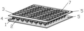
Fig.1. Perspective view of thermoelectric module according to present TEM.
Fig.2. Perspective view of spaced parts of thermoelectric module according to present TEM.
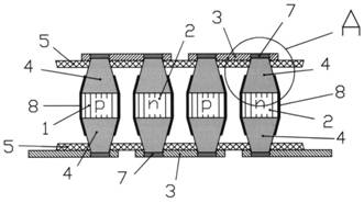
Fig.3.Cross section of thermoelectric module according to one embodiment of present TEM.
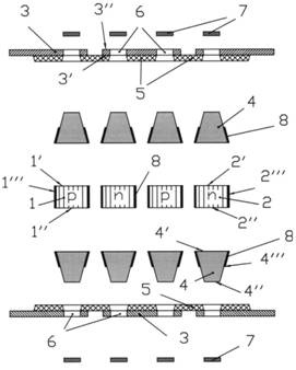
Fig.4.Cross section of thermoelectric module according to one embodiment of present TEM.
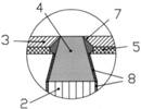
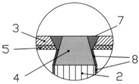
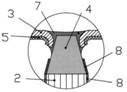
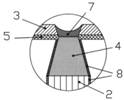
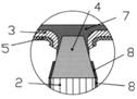
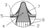
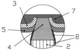
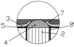
Fig.5.Different embodiments of place A in Fig.3.
As shown in Fig. 1-3 a thermoelectric module comprises thermoelectric semiconductor p-type elements 1, thermoelectric semiconductor n-type elements 2, which are arranged adjacent to each other, and plates 3 made of thermally and electrically conducting material.Each thermoelectric element 1, 2 (Fig. 4) has two equidistant surfaces 1', 1'' and 2', 2", and a side surface 1'" or 2"'. Each plate 3 (Fig. 4) has an inner surface 3' facing towards the ends of the thermoelectric elements and spaced from them (Fig. 3) and an outer surface 3" opposite to the surface 3' (Fig. 4).
The thermoelectric elements 1 and 2 and the plates 3(Fig. 3) are located between the intermediate elements 4 made of thermally and electrically conductive material such as copper and are permanently connected by its first ends 4' (Fig. 4) with the ends of respective thermoelectric elements 1 and 2. The layer of nickel or other metal (not shown in the drawings) disposes between each intermediate element 4 made of copper and the thermoelectric semiconductor element 1 or 2. This layer prevents cooper diffusion into material of thermoelectric elements. The second ends 4" of the intermediate elements are directed to the plates 3 and permanently connected with them (Fig.3 and 4). The cross-sectional area of the second end 4" (Fig.4) of each intermediate element at the connection with plate 3 is smaller than the cross-sectional area of the first end 4' connected with the end surface of respective thermoelectric element.
The inner surfaces 3' of the plates 3 are connected to the sheets 5 made of thermally and electrically insulating material (Fig.3 and 4).The through holes6 (Fig. 4) made in the plates 3 opposite of the thermoelectric elements 1 and 2. The sheets 5 have through holes (not denote in drawings) located opposite of said holes 6 of the plates 5. The second ends 4" of the intermediate elements 4 are permanently connected with plates 3 by means of connective thermally and electrically conductive material 7 inserted into the holes 6 (Fig. 3). The material 7 is the solder (in one embodiment), the copper (in another embodiment) or thermally conductive materials deposited by a vacuum deposition or electrochemically.
Sides 1"', 2"' of the thermoelectric elements 1 and 2 and partly of the intermediate elements 4 are covered by a layer 8 of thermally and electrically insulating material (Fig. 3 and 4).Figures 5 show embodiments of the place A (Fig.3) – connection of the intermediate elements 4 with plates 3.Intermediate elements 4 may be penetrate into the holes of the plates 3 (Fig.5). The second ends 4" of the intermediate elements 4 may be located at a distance from the outer surface 3' of the plates 3 (Fig.5).Thermally and electrically conductive material 7 may connect the side surfaces 4"' (Fig.4) of the intermediate elements 4 with plates 3 (Fig. 5).The holes 6 of the plates 3(Fig. 4) may have chamfers (not denote in drawings) on inside of the plates (Fig. 5) and on outer side of the plates (Fig. 5).The edges of the holes 6 in the plate 3 may be bent toward the outer surface of the plates 3 (Fig.5) or toward internal surface of the plates (Fig.5).The surfaces on the second ends 4" of the intermediate elements 4 or its positions may have a spherical shape (Fig.5). The connecting material 7 may connect the innersurfaces of the hole 6 and the side surface 4" of the intermediate elements 4 (Fig.5).The connecting material 7 may cover part of outer surface 3" of the plates 3 (Fig.5).The connecting material 7 may cover the entire outer surface 3" of the plates 3 (Fig.5).
Thermoelectric module may be manufactured by the following way.
At first the layers of nickel or other metal lay on the flat surfaces of the plate or flat washer made of thermoelectric semiconductor p-type or n-type material for preventing copper diffusion into said material. Then the layers of thermally and electrically conductive material such as copper lay on said surfaces above the layers of said metal preventing copper diffusion. Such half-finished product cut up into pieces having side surfaces which are perpendicular to flat surfaces of this half-finished product for obtaining plurality thermoelectric semiconductor elements which are permanently connected to intermediate elements. Simultaneously or sequentially the portions of the intermediate elements cut off for obtaining the cross-sectional area of the ends of the intermediate elements remote from the ends of the thermoelectric semiconductor elements being smaller than the cross-sectional area of the ends of intermediate elements connected with the ends surfaces of the thermoelectric semiconductor elements.
Then the side surfaces of the thermoelectric semiconductor elements and partly the surfaces of the intermediate elements cover by layers of the thermally and electrically insulating material. Simultaneously the plates of thermally and electrically conductive material and having holes which location corresponds to the position of thermoelectric semiconductor elements in the module are formed on the sheets made of thermally and electrically insulating material.
Alternately arranged thermoelectric semiconductor p-type and n-type elements with permanently connected intermediate elements collect to a package in which these elements are disposed adjacent to each other. Said sheets with said plates mount on this package of thermoelectric semiconductor elements with permanently connected intermediate elements. The thermally and electrically conductive material in form of the solder insert into holes of the plates from outer sides of the plates and subject it to heating or the outer surfaces of the plates cover by galvanically deposited copper.
If necessary, the outer surfaces of the plates may be cleaned of excess solder or galvanically deposited metal. If necessary, the surface of plate package treats to restore the flatness of the module. In addition may be provided necessarythickness of the module.The plates may be made from bimetallic electrically conductive material, e.g. clad aluminium.Plates and connecting thermally and electrically conductive material may be coated by thermally conductive and electrically insulating material such as aluminium oxide.
Plates made of thermally and electrically conductive material may be form by methods of planar plates forming after connection the thermoelectric semiconductor elements having permanently connected intermediate elements with the sheets made of thermally and electrically conductive material and having through holes.
In the thermoelectric devices, namely thermoelectric generators, thermoelectric cooling and heating devices the outer surfaces of plates made of thermally and electrically conductive material are connected to the heat transfer elements or such devices or are parts of the channels for passage of head-transfer fluid (not shown in the drawings). The electrical circuits formed by the plates 3, the intermediate elements 4 and the thermoelectric elements 1, 2, are connected to a consumer of electricity if device is the generator, or connected to a power source if device is the cooling and heating device (not shown in the drawings).
Technological and raw-stuff restrictions. Technological restrictions are the high cost of an assembly of TEM, temperature limit of TEM operating mode associated with the presence of solder in the construction, and restrictions of planar dimensions due to arising of thermo-mechanical stresses in TEM during its operation.
Specificity of TEM is that during the operation process module experiences not only significant and sudden changes in temperature, but also considerable internal temperature gradients.For TEG must be considering thermo-mechanical stresses not only on a scale of the whole structure, but also on a scale of the each thermocouple leg.To illustrateproblems of TEM manufacturing, below have shown a small in size number of dependencies.
In order to achieve a high conversion efficiency or the maximum coefficient of performance (COPmax = Qх/Wconsumption) at a predetermined electric voltage it is crucial that TEMhas a certain number of series-connected pairs of legs (N(p-n)), which depends on the difference in temperature between the thermocouple junctions (Fig. 6).
The maximum coefficient of performance increases while reducing the temperature difference (COPmax=Wc/W(I∙V)), but this increases the optimal number of series-connected thermocouple legs (N(p-n)),and at the same time it decreases the total cooling capacity of thermocouples (Wc).
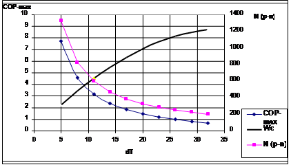
Fig.6.Dependenceofoptimal number of thermocouple legs on ∆Т for Z(p-n) = 2,6•10-3K-1.
In order to ensure a high total cooling capacity it is necessary to increase the total number of thermocouples in TEM or reduce the height of the thermocouple legs in TEM.Reducing the height of the thermocouple legs reduces their thermoelectric efficiency (Fig.7),it may, however, be noted that we consider it in the calculation basis.We have the capability of reducing of the height of thermocouple legs to a sizeof 0.2mm (the most frequently used thermocouple legs with a height of 1 mm, but the flow rate of the material in this case is 25 times more).
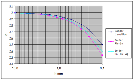
Fig. 7.Dependence of thermoelectric efficiency (Z•103K-1) onheight of thermocouple legs and applied solder.
- ρcu=2•10-6 [Оhm∙сm] (galvanically deposited copper)
- ρPb-Sn=17•10-6 [Оhm∙сm]
- ρSn-Cu-Ag=12•10-6 [Оhm∙сm]
Reducing the height of the thermocouple legs would significantly reduce the consumption of the thermoelectric material, but at the same time reducing the height leads to a substantial increase of the thermomechanical stresses inTEM (Fig.8).The same result has obtained by increasing the total number of the thermocouple legs in TEM in view of the fact thatthe planar dimensions ofTEMare increasing.
In principle, this problem could be solvingthrough the use of the thermocouple legs with a low height and small cross section. However, such a solution to reduce thermomechanical stresses, and such savings of raw material lead to an increase in production costs and decrease reliability and efficiency.
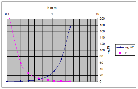
Fig.8.Dependence of content of thermoelectric material in TEM and thermomechanical stresses in TEM on height ofthermocouple legs.
Thermomechanical stresses in TEM described by the formula:
σ = 6·α·∆Т·L·Е·А/H2
Where ΔТ=Тh -Тc is the temperature difference between the hot and cold ceramic plates of TEM;
α – Temperature coefficient of linear expansion of the ceramic plates;
Е – Young's modulus (also known as the tensile modulus or elastic modulus);
L, A, H – shown in the Fig.9.
For the square TEM:
L – Distance between the outer legs of the thermocouple located diagonally;
А – Length of the diagonal cross-section of the thermocouple leg (for square and round legs are respectively cross-sectional diagonal and diameter of thermocouple legs).
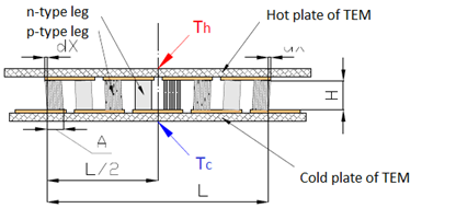
Fig.9.Illustration of thermomechanical deformations of TEM.
Above reasons, explains: High cost of TEM; Thermoelectric material flow per watt of produced power ofthe cold or electricity generation; Low level of reliability;Weight and size characteristics.
CONCLUSIONS
Thermoelectric modules in agriculture let improve efficiency of equipment and significantly reduce loss of energy. Furthermore, application of nano structured TEM for milk thermoelectric coolers are a friendly approach to the environment and farm animals.
It is necessary to define what kind of skills and knowledge are needed to take advantage of nanotechnology and to manage risks that are likely to emerge with increasing commercialization of products, created on the ground of applications of nanotechnologies.
It is necessary to define export potential of new type of thermoelectric generators, thermoelectric cooling and heating devices, to create in Latvia a research infrastructure for the next generation TEM development.
Elaborated the new type of thermoelectric modules may be used in thermoelectric generators, thermoelectric cooling and heating devices.
The new TEM production technology improved consumer properties of TEM: temperature resistance, resistance to cyclic loads, increased efficiency (COP); thenew type of thermoelectric modules reduces the consumption rare earth elements in TEM (g/W) by 80% and reduces the cost and consumption of material for TEM by 50%.
2. Miller Edwin et al, Patent of USA Nr. 3 279 955 A, 1966;
3. Maekawa Nobuteru et al, Patent of USA Nr. 5 841 064 A,1998;
4. BelovY.Patent of Russia No.2511274 "A Thermoelectric Module",2014;
Aleksandrs Homko, Genadijs Moskvins DEVELOPMENT OF NANOSTRUCTURED THERMOELECTRIC MODULES FOR AGRICULTURE
. International Journal Of Applied And Fundamental Research. – 2014. – № 2 –
URL: www.science-sd.com/457-24700 (06.07.2025).